Semiconductor Process Material Specifications: Purity, Coatings & Certifications for Critical Fab Components
Semiconductor Process Material Specifications: Purity, Coatings & Certifications for Critical Fab Components
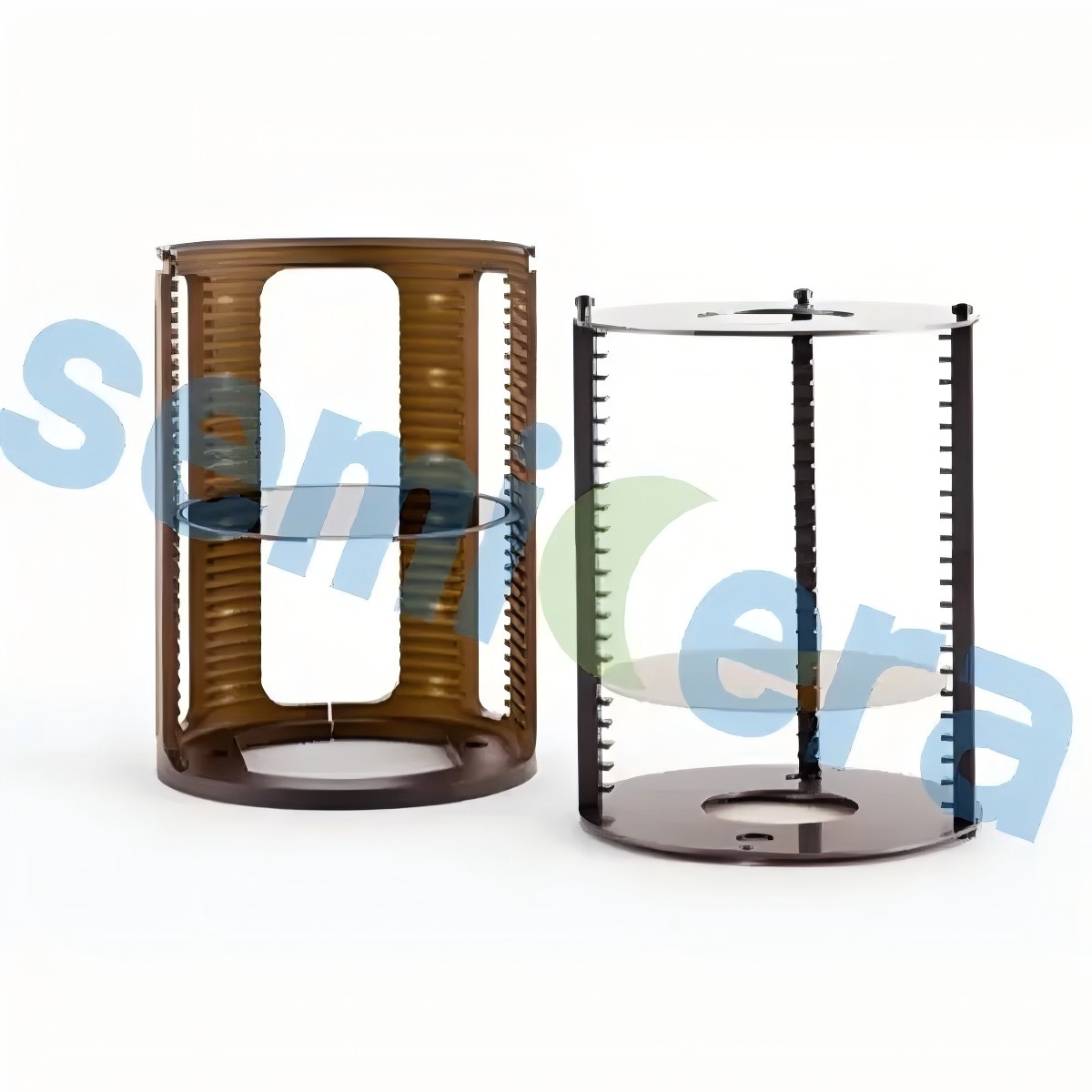
The global semiconductor materials market reached $67.5 billion in 2024, driven by increasing demand for advanced chips and tighter process tolerances. For procurement and process engineers evaluating semiconductor process materials, understanding the interplay of purity grades, coating technologies, and certifications is essential to avoid yield losses and equipment downtime. This guide provides a structured breakdown of the key specifications that define usable process components, with a focus on products from Semicera (Ningbo Miami Advanced Material Technology Co., LTD), a manufacturer with over 600 employees and a 40,000 m² facility dedicated to semiconductor hot-zone and consumable parts.
Why Material Specifications Matter in Semiconductor Manufacturing
In epitaxy (MOCVD), etching, diffusion, and crystal growth, process materials must withstand extreme temperatures (up to 2,200°C), corrosive gases (NH₃, H₂, CF₄), and stringent purity requirements. A component with an ash content above 5 ppm or a coating that delaminates under thermal cycling can contaminate wafers, causing scrap. Therefore, buyers moving from research to evaluation need a clear framework to assess candidate materials.
Key Product Families and Their Critical Parameters
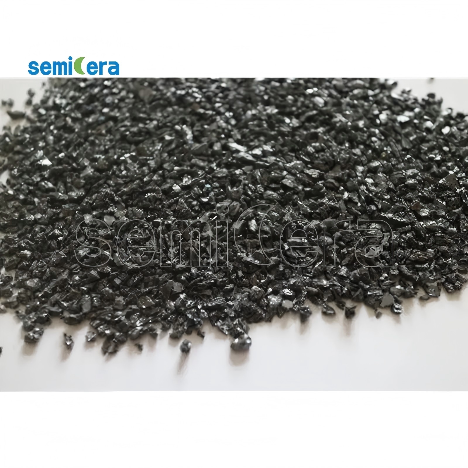
The following table summarizes the core product categories from Semicera, with parameters extracted from verified datasheets. Each product is designed for a specific process environment, and the selection depends on temperature, gas chemistry, and mechanical load.
| Product Category | Key Material | Purity / Ash Content | Max Working Temperature | Key Coating / Feature | Primary Process |
|---|---|---|---|---|---|
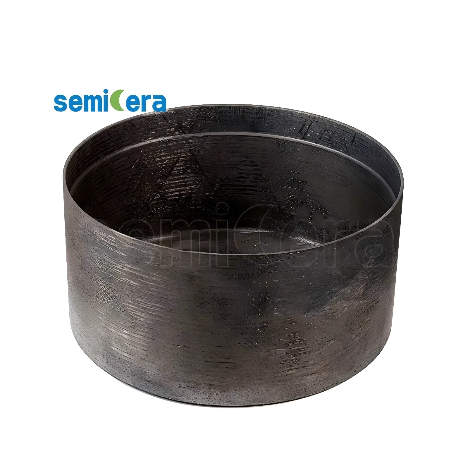
| Semiconductor graphite | Isostatic graphite | Ash ≤ 5 ppm | Depends on coating | Ultra-fine grain (2–5 µm), CTE 4.0–4.6×10⁻⁶ K⁻¹ | General hot-zone base |
| CVD SiC coating graphite carrier (CVD-01) | Graphite + CVD SiC | 99.99995 % (6N), ash ≤ 5 ppm | Coating survives >1600 °C | β-SiC (111), 100 µm typical, 2500 HV | Epitaxy / RTP |
| CVD TaC coating graphite carrier (CVD-02) | Graphite + CVD TaC | High-purity TaC | 2200 °C | TaC cubic, 25–45 µm, NH₃/H₂ resistant | SiC/GaN epitaxy |
| CFC material | Carbon‑carbon composite | Ash ≤ 10 ppm after halogen purification | >2000 °C | 2.5D/3D needle‑punched, tensile 90–140 MPa | Crystal growth hot‑zone |
| SiC wafer boat (SiC-01) | SiSiC / RSiC | 99.9 % | 1600 °C | Life >5× quartz boats, 1000 °C → RT cycling | Diffusion / oxidation |
| Quartz furnace tube | Fused quartz (OH < 20 ppm) | SiO₂ ≥ 99.99 % | 1150 °C cont., 1300 °C short | Bubble‑free, OD tolerance ±1 % | Oxidation / LPCVD |
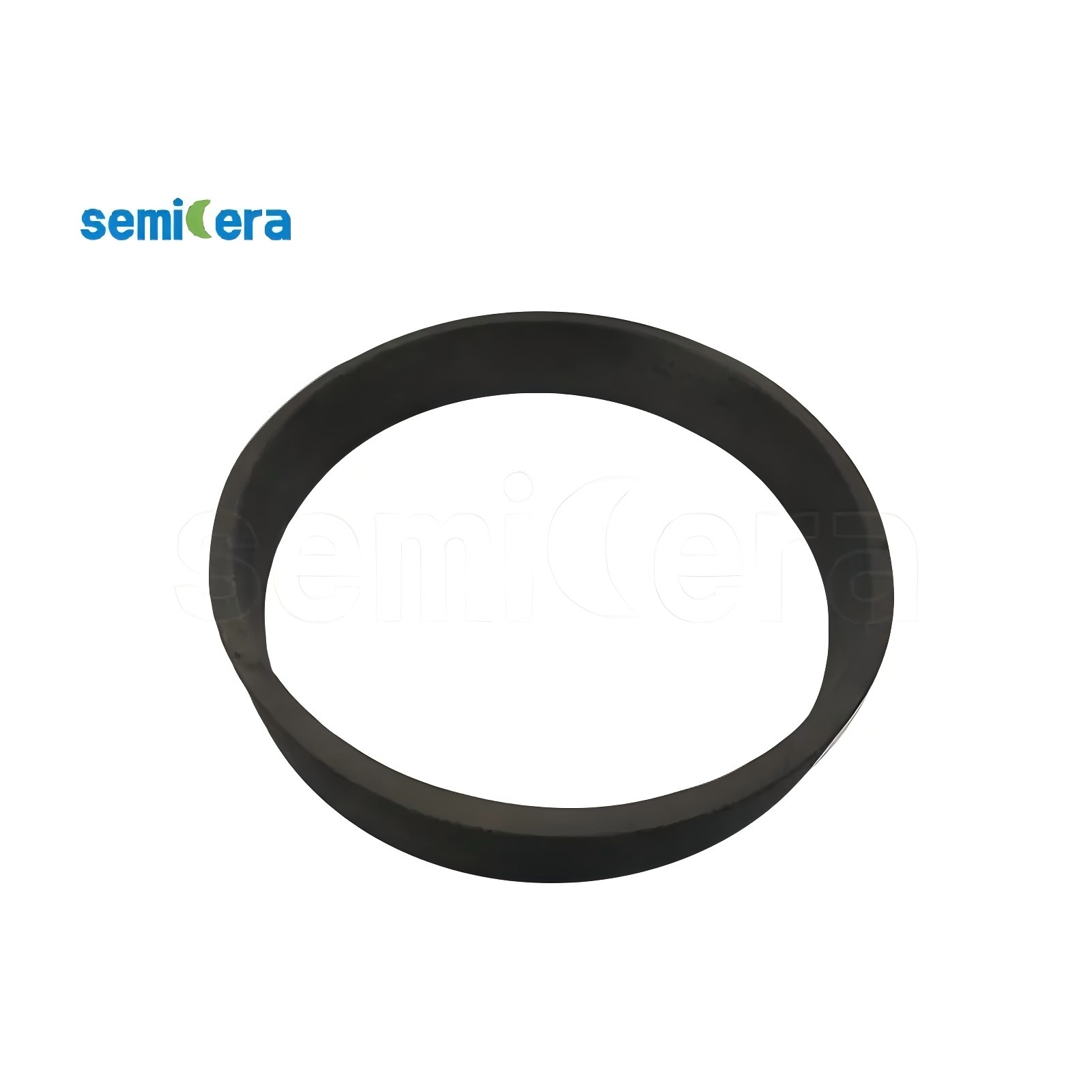
| Etch ring | CVD solid SiC | Total metals < 5 ppb | N/A (plasma) | Plasma erosion < 2 nm/min, flatness ≤ 10 µm | RIE / ICP etch |
Certifications: What Is Covered?
Semicera’s semiconductor process materials carry the following quality management certifications, each verified for specific product IDs:
- ISO 9001 (Quality Management) – covers CVD SiC coating graphite carrier (ID 4919), CFC material, semiconductor graphite (ID 4932), SiC wafer boat (ID 4926), SiC furnace tube (ID 4927) and others.
- ISO 14001 (Environmental Management) – covers the same portfolio, including semiconductor graphite (ID 4932) and CVD SiC coating carrier.
- ISO 45001 (Occupational Health & Safety) – covers graphite products (ID 4932) and coating carriers (ID 4919).
All certifications are issued by ISO and are applicable globally, ensuring that every exported batch meets internationally recognized standards.
Step-by-Step: Matching Material to Process
- Identify process regime: For MOCVD epitaxy (NH₃/H₂, >1600 °C), choose TaC-coated graphite (CVD-02) or SiC-coated graphite (CVD-01). For SiC crystal growth (PVT, >2000 °C), CFC heaters and CVD solid SiC parts offer the needed thermal stability.
- Define purity budget: If metal contamination tolerance is below 1 ppm, require 6N+ grade CVD SiC particles (CVD-04) for raw material or solid CVD SiC components.
- Evaluate coating integrity: Demand coating thickness uniformity (e.g., ±10 µm for SiC, ±5 µm for TaC), no peeling under 1000 °C cycles, and hardness > 2500 HV for plasma resistance.
- Confirm certifications: Request ISO 9001/14001/45001 certificates to validate the supplier’s quality management system and product traceability.
Real-World Performance: Case Highlights
- A North America client used Semicera’s SiC wafer boats (900 units/month) for epitaxy. Over two years, the boats delivered stable mass production and reduced equipment maintenance downtime by 15 %.
- A Korea client running CVD SiC coated graphite carriers (500 pcs/month) for epitaxy saw edge ring replacement frequency drop by 20 %, attributed to the coating’s resistance to fluorine/chlorine plasma.
- A Taiwanese client applied CFC material for silicon single‑crystal furnace insulation (1000 units/year). The 3D needle‑punched composite maintained zero structural deformation over two years, leading to significant energy efficiency gains.
Frequently Asked Questions
- What certifications are available for semiconductor process materials? Semicera’s critical semiconductor components are certified under ISO 9001, ISO 14001, and ISO 45001. These apply globally to products including CVD SiC coating carriers, semiconductor graphite, SiC wafer boats, and SiC furnace tubes. Certificates are issued by ISO and are valid through December 2026.
- What purity levels can be achieved for graphite‑based materials? Isostatic graphite blocks used as substrates have an ash content ≤ 5 ppm. CVD SiC coatings reach 99.99995 % (6N grade, total ash ≤ 5 ppm). For raw SiC crystal growth material, CVD SiC particles offer ≥ 99.9999 % (6N+, total metals < 1 ppm).
- How does the cost‑benefit compare between coated and uncoated components? While coated carriers cost initially more, they extend service life significantly. For example, SiC wafer boats last more than 5× longer than quartz boats, and CVD TaC coatings protect against NH₃/H₂ etching at 2200 °C, reducing replacement frequency. No exact price data is available, but the total cost of ownership is lower over a multi-year horizon.
- Can I request samples for qualification? Semicera supports OEM production with a monthly capacity of 10,000+ units and a minimum order quantity of 1 unit. Samples can be arranged for process qualification. Contact the sales team to discuss your specific application.
- What is the typical lead time? For standard semiconductor graphite parts and coated carriers, the lead time is 30–50 days from order confirmation. Custom designs may require additional engineering time.

To obtain a detailed catalog with complete technical datasheets for all Semicera semiconductor process materials, please download the company brochure or reach out to the global sales team via WhatsApp or email.
Have Questions or Need More Details?
Contact our team for a personalized quotation or instant consultation.
Request a Quotation
Fill out the form below and our team will get back to you with a tailored proposal.
WhatsApp Direct Chat
Prefer to chat in real-time? Message us on WhatsApp for instant assistance & quick answers.
- Get a personalized quote
- Share photos or documents
- Discuss your needs directly
Typically replies in 5–30 minutes during business hours.