
Semiconductor Process Materials Guide: Materials, Applications & Selection
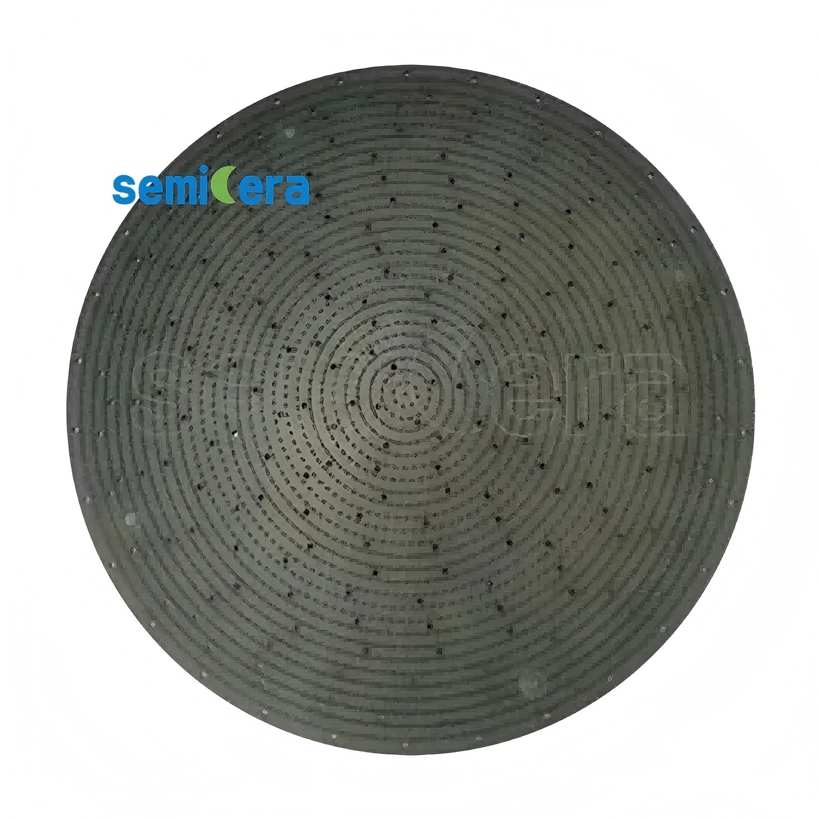
Semiconductor Process Materials Guide: Materials, Applications & Selection
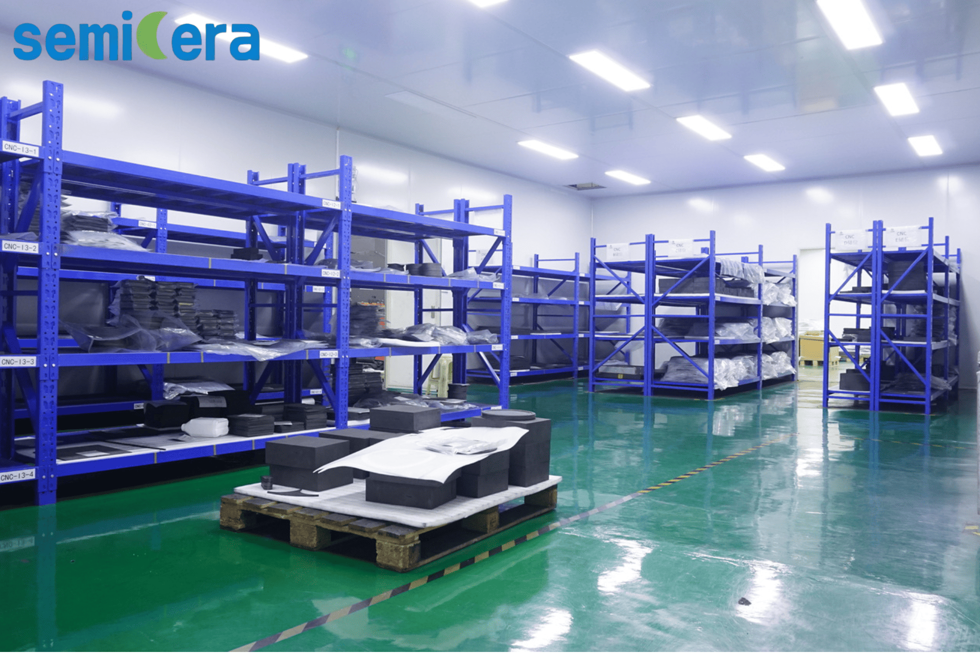
Semicera (Ningbo Miami Advanced Material Technology Co. LTD), established in 2015, specializes in designing and manufacturing high-purity semiconductor materials and components. The company operates dual research centers and three large-scale production bases, employing approximately 600+ staff with a manufacturing facility covering 40,000 m². Semicera’s product portfolio covers the entire spectrum of semiconductor process materials—from high-purity isostatic graphite and carbon‑carbon composites to CVD SiC, TaC, and PyC coated parts as well as quartz and ceramic components. These materials are used in critical steps such as epitaxy, etching, crystal growth, oxidation, and diffusion.
Why Semiconductor Process Materials Matter
Semiconductor manufacturing relies on materials that can withstand extreme temperatures, corrosive gases, and ultra‑high vacuum without introducing contamination. A single impurity particle or a 5 ppm ash level can ruin an entire batch of wafers. Selecting the right process material—whether a graphite susceptor, a quartz furnace tube, or a SiC wafer boat—directly affects yield, throughput, and tool uptime.
The global semiconductor materials market reached $67.5 billion in 2024 (SEMI), with wafer fabrication materials (including process chemicals and CVD materials) accounting for $42.9 billion. Within this, the semiconductor graphite market alone was valued at approximately $1.62 billion in 2024 (Verified Market Reports). As device nodes shrink and new materials like SiC and GaN gain adoption, the demand for ultra‑pure, thermally stable, and chemically resistant process materials is growing.
Semicera’s Comprehensive Product Line
Semicera supplies semiconductor process materials across multiple categories, each engineered for specific process conditions. Below is an overview of the key product families.
1. High‑Purity Isostatic Graphite
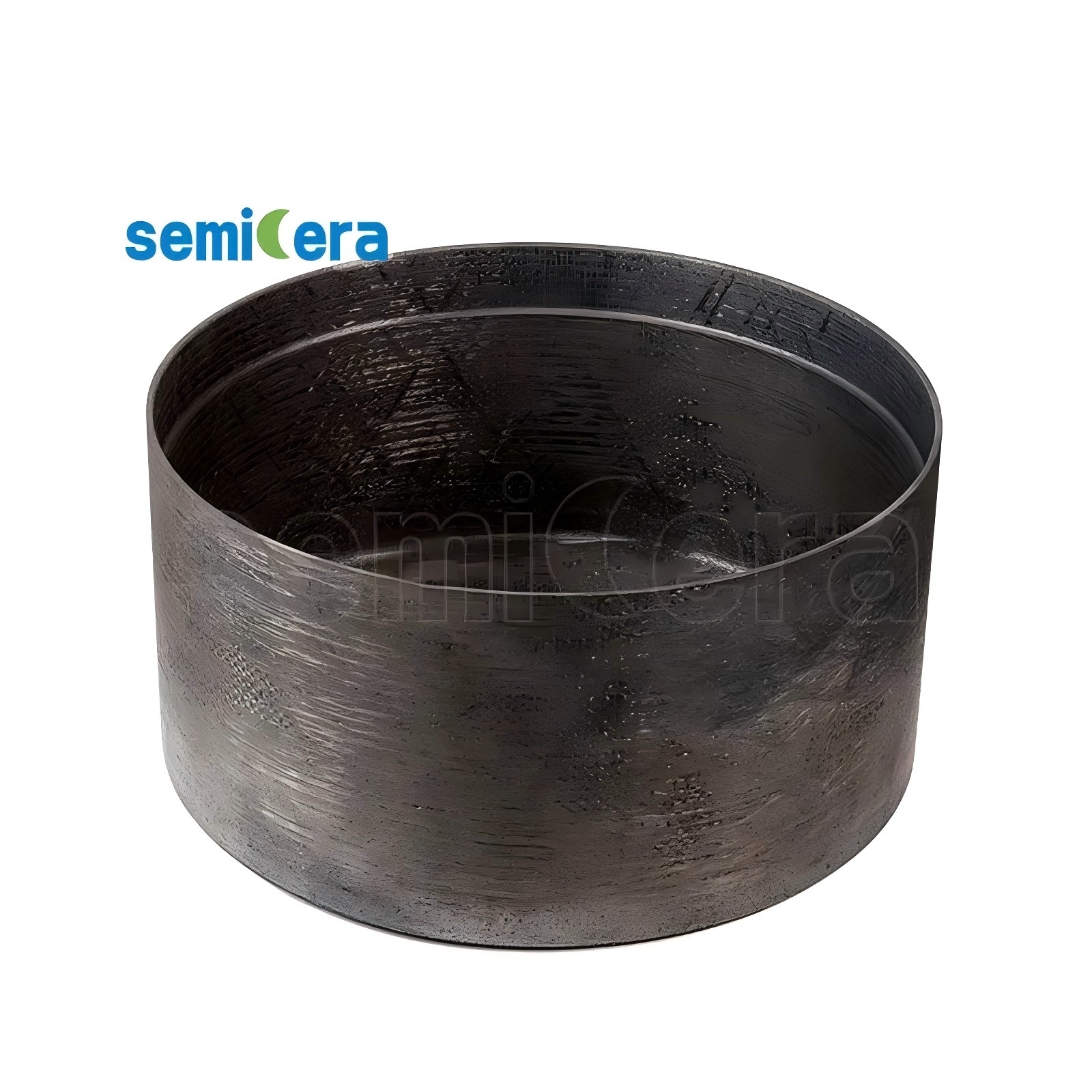
Model designation: Semiconductor graphite – supplied as blocks or machined parts. It uses ultra‑fine grain size (2–5 µm) with ash content ≤5 ppm (semiconductor ultra‑pure grade), flexural strength 45–65 MPa, and a coefficient of thermal expansion of 4.0–4.6×10⁻⁶ K⁻¹. This material serves as the base for hot‑zone components, susceptors, heaters, and structural parts in ingot furnaces, epitaxial reactors, and other thermal processes.
2. Carbon‑Carbon Composite (CFC)
Model designation: CFC material – a 2.5D or 3D needle‑punched carbon fiber composite with tensile strength 90–140 MPa. After halogen purification, ash content is kept ≤10 ppm. CFC components (heaters, bolts, crucibles) provide lightweight, high‑strength support in crystal growth furnaces (CZ/PVT) where severe thermal shock and mechanical rotation occur at temperatures above 2000°C.
3. CVD SiC Coated Graphite Carriers
Model CVD-01 – MOCVD multi‑pocket wafer susceptor/tray with a beta‑phase polycrystalline SiC coating (FCC, (111) oriented). Typical coating thickness: 100 µm (range 50–150 µm). Purity: 99.99995% (6N grade, total ash ≤5 ppm). Coating hardness: 2500 Vickers (40 GPa). These carriers are the industry standard for epitaxial reactors and RTP systems where thermal uniformity and low particle generation are critical.
4. CVD TaC Coated Graphite Carriers
Model CVD-02 – cubic tantalum carbide (TaC) matrix coating on graphite, typically 25–45 µm thick. Maximum operating temperature: 2200°C. TaC offers outstanding resistance to ammonia (NH₃) and hydrogen (H₂) etching, making it indispensable for ultra‑high‑temperature SiC and GaN epitaxy.
5. CVD Solid SiC Parts
Model CVD-03 – 100% bulk solid CVD SiC (zero substrate), density ≥3.21 g/cm³, thermal conductivity ≥150 W/m·K, zero porosity. Used as dummy wafers, etch rings (focus rings) for plasma etchers, and other chamber components. With total metal impurity <5 ppb and plasma erosion rate <2 nm/min (CF₄/O₂), these parts excel in etch and cleaning processes.
6. Silicon Carbide (SiC) & Quartz Components for Oxidation/Diffusion
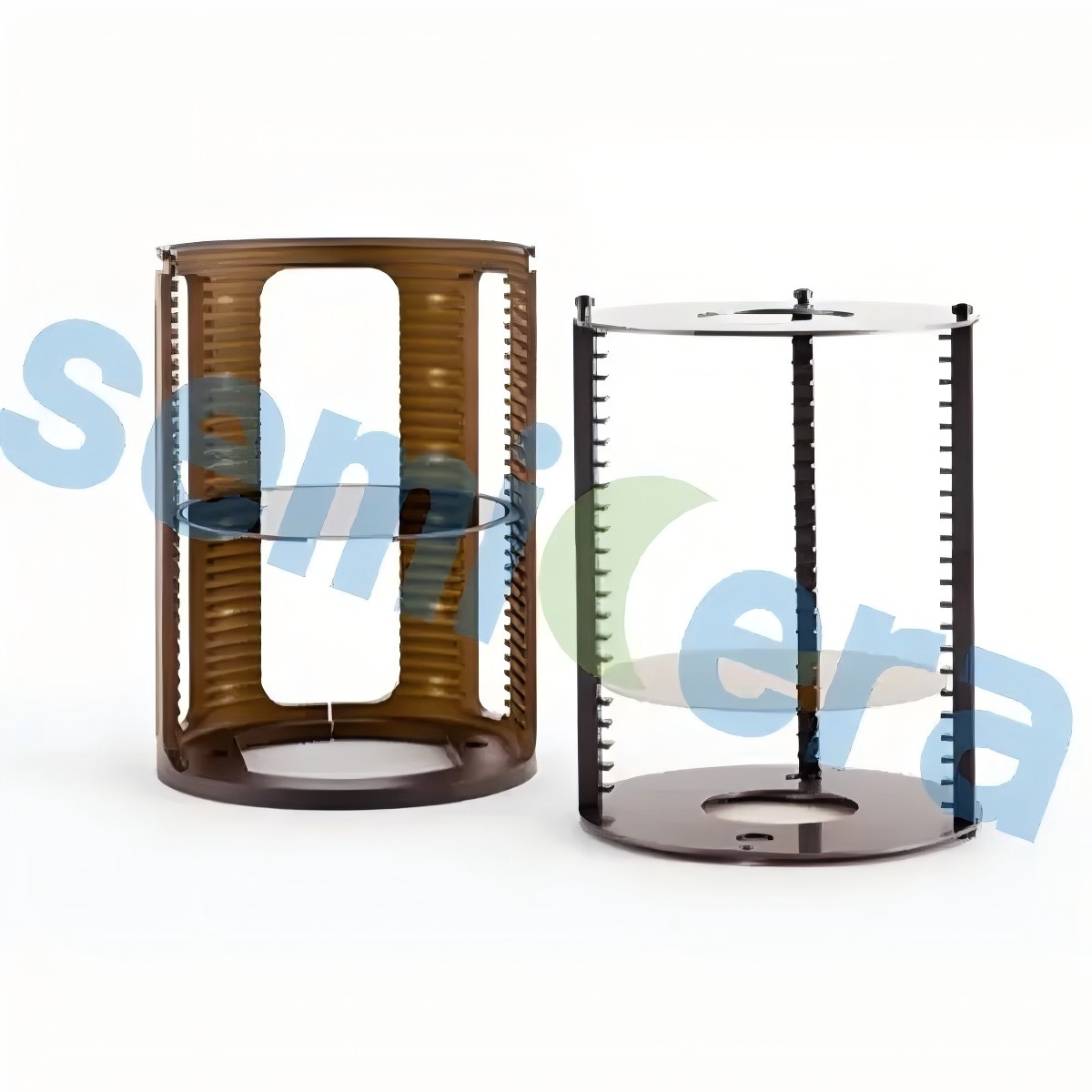
Semicera’s SiC wafer boat (model SiC-01) is a sintered/re‑crystallized SiC diffusion boat that can withstand 1600°C with zero structural deformation, delivering >5× longer service life than traditional quartz boats. The SiC furnace tube (model SiC-02) is an LPCVD/high‑temperature oxidation process tube made of CVD SiC coating on SiSiC, impermeable to gases, with length up to 3000 mm and wall thickness uniformity ±0.2 mm. For lower‑temperature applications, the quartz furnace tube (OH content <20 ppm) and quartz wafer boat (GE214 grade, SiO₂ ≥99.99%) provide clean reaction chambers at 1150°C continuous / 1300°C short‑term.
7. Thermal Insulation: Soft & Rigid Felt
For crystal growth hot‑zone insulation, Semicera provides flexible purified graphite felt (carbon content ≥99.99%, moisture <1%) and rigid carbon board (ash ≤20 ppm standard, ≤5 ppm ultra‑grade). These felts and boards maintain thermal uniformity and energy efficiency in Czochralski and PVT furnaces.
8. High‑Purity CVD SiC Raw Material
Model CVD-04 – Polycrystalline SiC particles (1.0–5.0 mm, 6N+ purity, free carbon ≤0.05 ppm) used as source material for PVT crystal growth. Bulk density close to 3.21 g/cm³ ensures consistent sublimation behavior.
Step‑by‑Step: How to Select the Right Semiconductor Process Material
- Identify the process window – temperature range, gas chemistry (oxidizing/reducing/plasma), vacuum level.
- Determine purity requirements – for <5 ppm ash, ultra‑fine grain isostatic graphite or CVD SiC coating is necessary; for <1 ppb metals, bulk CVD SiC or TaC coating is preferred.
- Evaluate mechanical stress – high‑load cantilever applications (e.g., SiC paddle) demand sintered RSiC core with deflection ≤2.0 mm at 2000 mm reach.
- Check coating compatibility – SiC coating for general epitaxy; TaC coating for NH₃/H₂ aggressive ambient; PyC coating for specific insulation or chemical barrier needs.
- Validate dimension and tolerance – wafer boats require slot pitch ≤±0.05 mm; etch rings need flatness ≤10 µm.
- Request sample testing – engage the supplier to provide test coupons or pilot runs that simulate actual process conditions.
Application‑Specific Use Cases
Epitaxy & MOCVD
CVD SiC coated graphite susceptors (CVD-01) are used in MOCVD reactors for LED and power device epitaxy. Where GaN or SiC epitaxy demands higher temperatures (>1600°C) and ammonia resistance, TaC coated carriers (CVD-02) are the preferred solution.
Etch (Plasma)
Etch rings (focus rings) made of CVD solid SiC or high‑purity silicon single crystal protect chamber walls and focus plasma on the wafer edge, with total metal impurity <5 ppb and erosion rate <2 nm/min. Bulk CVD SiC components (CVD-03) serve as chamber liners and dummy wafers.
Crystal Growth (Si & SiC)
CFC crucibles and heaters, along with rigid/felt insulation, form the hot zone of Czochralski and PVT furnaces. High‑purity CVD SiC particles (CVD-04) act as feedstock for PVT SiC boule growth.
Oxidation / Diffusion / LPCVD
SiC furnace tubes (SiC-02) and SiC wafer boats (SiC-01) replace quartz in high‑temperature LPCVD and oxidation processes, offering longer life and better thermal shock resistance. Quartz furnace tubes and boats remain cost‑effective for lower‑temperature (<1150°C) applications.
Material Comparison Table
| Property | Isostatic Graphite | CFC | CVD SiC Coated Graphite | CVD TaC Coated Graphite | CVD Solid SiC | Quartz (Fused) |
|---|---|---|---|---|---|---|
| Max Temp (°C) | ~2500 (inert) | >2000 (inert) | ~1600 (SiC coating) | 2200 | >1600 | 1150 cont./1300 short |
| Ash / Purity | ≤5 ppm | ≤10 ppm | ≤5 ppm (coating 6N) | High‑purity TaC | <1 ppm metals | SiO₂ ≥99.99% |
| Mechanical Strength | Flexural 45–65 MPa | Tensile 90–140 MPa | Coating hardness 2500 HV | – | Density ≥3.21 g/cm³ | GE214 grade |
| Primary Use | Hot‑zone base, susceptors | Heaters, crucibles | MOCVD susceptors, RTP | Ultra‑high temp epitaxy | Etch rings, dummy wafers | Furnace tubes, boats |
| Resistance to Corrosion | Oxidizes in air >500°C | Oxidizes; halogen‑purified | Excellent vs. H₂/Cl₂ | Excellent vs. NH₃/H₂ | Extreme plasma & chemical | Good vs. most acids |
Frequently Asked Questions
Purity depends on the specific process. For hot‑zone graphite, ash content ≤5 ppm is the semiconductor ultra‑pure grade. CVD SiC coating parts achieve 99.99995% (6N, ash ≤5 ppm). For the most demanding etch applications, CVD solid SiC has total metal impurity below 5 ppb. This ensures minimal contamination during wafer fabrication.
Semicera provides three types of chemical vapor deposition (CVD) coatings on graphite: SiC (beta‑phase, FCC, typical 100 µm), TaC (cubic tantalum carbide, 25–45 µm), and PyC (pyrolytic carbon). Each coating is optimized for specific process gases and temperatures—SiC for general epitaxy, TaC for ultra‑high‑temperature ammonia environments, and PyC for specialized thermal barriers.
Semicera’s SiC wafer boat (model SiC-01) offers a service lifespan more than five times that of traditional quartz boats. Although the initial cost is higher, the extended life and zero‑deformation performance at up to 1600 °C reduce total cost of ownership, especially in high‑temperature LPCVD and oxidation processes where quartz would degrade quickly.
Yes. The company supplies semiconductor graphite as blocks or machined parts with ultra‑fine grain size and tight tolerances. CFC components can also be machined to customer drawings. With three production bases and more than 50 advanced production lines, Semicera can handle custom shapes for heaters, crucibles, bolts, and structural hot‑zone parts.
Lead time varies by order volume and coating thickness. As a manufacturer with an annual output of 120,000 units and 600+ employees, Semicera maintains production capacity for standard susceptor sizes. For specific lead‑time and availability, contact the sales team with your process requirements and target quantity. Contact Semicera for a quote or sample request.
For detailed specifications, sample requests, or a customized quote, email sales05@semi-cera.com or message via WhatsApp: +86 15957878134.
Have Questions or Need More Details?
Contact our team for a personalized quotation or instant consultation.
Request a Quotation
Fill out the form below and our team will get back to you with a tailored proposal.
WhatsApp Direct Chat
Prefer to chat in real-time? Message us on WhatsApp for instant assistance & quick answers.
- Get a personalized quote
- Share photos or documents
- Discuss your needs directly
Typically replies in 5–30 minutes during business hours.