Semiconductor Process Material Decision Guide: CFC vs Graphite vs SiC/TaC-Coated Parts
Semiconductor Process Material Decision Guide: CFC vs Graphite vs SiC/TaC-Coated Parts
For semiconductor manufacturers and equipment buyers, selecting process materials is a technical and financial decision, not just a purchasing activity. The practical question at this stage is not “which material is the most advanced” but “which material system delivers the lowest total cost of ownership for our specific process.”
This guide compares two documented material choices for high-temperature semiconductor manufacturing. The first is CFC material, a carbon-fiber-reinforced carbon composite, compared with conventional solid graphite hot-zone components. The second is SiC/TaC-coated components compared with original equipment manufacturer (OEM) parts.
The comparison evidence from Semicera shows that CFC material provides 3 to 5 times longer service life, over 20% higher structural load capacity, and up to 50% better energy efficiency than conventional solid graphite. SiC/TaC-coated parts offer 30–40% lower cost than OEM parts with the same lifespan, a 10–15% improvement in epitaxial layer uniformity, and less than 5% particle generation. The sections below explain when these differences matter and how to apply them in a decision framework.
Problem Definition: Why the Material Comparison Matters
Semiconductor process materials cover high-purity components used inside wafer fabrication equipment: graphite susceptors, SiC wafer boats, quartz furnace tubes, hot-zone materials, and coated parts for epitaxy, annealing, etch, and crystal growth processes. These components operate under high temperature, reactive gases, and strict purity requirements.
A wrong material decision can show up as coating cracking, outgassing, particle contamination, and defects on the epi layer. In crystal growth, it can appear as poor thermal uniformity, higher energy consumption, and shorter component life.
At the decision stage, buyers compare three things: technical performance, total cost over the component’s life, and supplier ability to control quality consistently. Price-per-part is only one input. The more relevant comparison is cost per wafer, per run, or per year of operation.
For this reason, a material comparison should be built on measurable attributes: service life, structural load capacity, energy efficiency, epitaxial layer uniformity, particle generation, and defect density.
Industry Background: A Growing and More Demanding Material Category
The semiconductor materials market is expanding, and the demand for high-performance process materials is growing with it.
According to SEMI, the global semiconductor materials market reached $67.5 billion in 2024, an increase of 3.8% from the previous year. Wafer fabrication materials, which include process chemicals and CVD materials, increased 3.3% to $42.9 billion in 2024.
Within this category, three segments are directly relevant to hot-zone and coating decisions:
- The global semiconductor graphite market was valued at approximately $1.62 billion in 2024 and is projected to grow at a CAGR of 7.2% through 2032, according to Verified Market Reports.
- SiC-coated graphite susceptors, critical for epitaxial growth, were valued at approximately $350 million in 2024, according to Valuates Reports.
- The global market for quartz fabricated parts used in semiconductor manufacturing reached approximately $2.21 billion in 2024, with 5.5% annual growth, according to TECHCET.
CVD SiC coating is widely recognized as the dominant protection method for graphite susceptors in MOCVD and epitaxial reactors. Tantalum carbide (TaC) coatings are also gaining traction for ultra-high-temperature processes such as SiC crystal growth.
For procurement teams, these trends mean two things: more material options are available, and the financial impact of the decision is larger. A structured comparison is therefore necessary.
Detailed Solution: Two Comparison Sets That Support the Buying Decision
Comparison 1: CFC Material vs Conventional Solid Graphite Hot-Zone Components
CFC material is a carbon-fiber-reinforced carbon composite used for hot-zone components in high-temperature furnaces. Compared with conventional solid graphite, Semicera’s CFC material offers three important performance differences:
- Service life: 3 to 5 times longer under continuous high-temperature pulling conditions.
- Structural load capacity: over 20% higher than solid graphite.
- Energy efficiency: up to 50% better than solid graphite.
The result is a lower total cost of ownership. Extended component lifespan reduces the frequency of replacement, and reduced maintenance requirements lower operating cost.
This combination makes CFC material more suitable for silicon crystal growth process scenarios, where furnaces operate for long periods at high temperature and component changes are expensive.
An important observation for buyers: CFC material may have a similar purchase cost to solid graphite. The advantage comes from lifecycle performance, not from a lower initial price.
Comparison 2: SiC/TaC-Coated Components vs OEM Parts
SiC/TaC-coated components are graphite parts with a CVD-applied silicon carbide or tantalum carbide coating. They are designed for processes where surface purity and particle control are critical, especially epitaxy.
Compared with OEM parts, Semicera’s SiC/TaC-coated parts show the following differences:
- Cost: 30–40% lower than OEM parts.
- Lifespan: same service cycle and maintenance interval as original OEM components.
- Epitaxial layer uniformity: 10–15% improvement over OEM parts.
- Particle generation: less than 5%, compared with OEM parts.
- Defect control: minimized defect density due to ultra-pure CVD SiC coating, which prevents outgassing and particle contamination.
For an epi process, these attributes directly affect yield. Better uniformity means more consistent layer thickness across the wafer. Lower particle generation reduces pits, micropipes, and other epi-layer defects.
The cost advantage is substantial: buyers are not choosing between a low-cost part and a high-quality part. They are choosing a part that costs less, lasts the same, and improves a measurable process outcome.
Step-by-Step Decision Framework for Buyers
To turn these comparison points into a defensible purchasing decision, use the following five-step framework.
Step 1: Define the Process and Thermal Profile
Identify where the component will operate. Silicon crystal growth, epitaxy, MOCVD, and other high-temperature processes have different thermal and purity requirements. CFC material is more suitable for crystal growth. SiC/TaC-coated parts are more suitable for epitaxy.
Step 2: Identify the Primary Failure Mode
Ask what can go wrong. In crystal growth, the main risk is thermal fatigue and component degradation. In epitaxy, the main risks are outgassing, particle contamination, and coating cracking. The material choice should address the dominant risk first.
Step 3: Compare Performance with the Same Metrics
Use a single set of metrics: service life, structural capacity, energy use, uniformity, particle count, and maintenance interval. Avoid comparing a supplier’s “quality” in general terms; ask for numbers.
Step 4: Calculate Total Cost of Ownership, Not Just Unit Price
TCO = purchase price + maintenance cost + energy cost + downtime cost over the component’s life. A component with 3 to 5 times longer life can justify a higher initial price. A component with the same life and a 30–40% lower price creates immediate savings.
Step 5: Verify the Supplier’s Manufacturing and Testing System
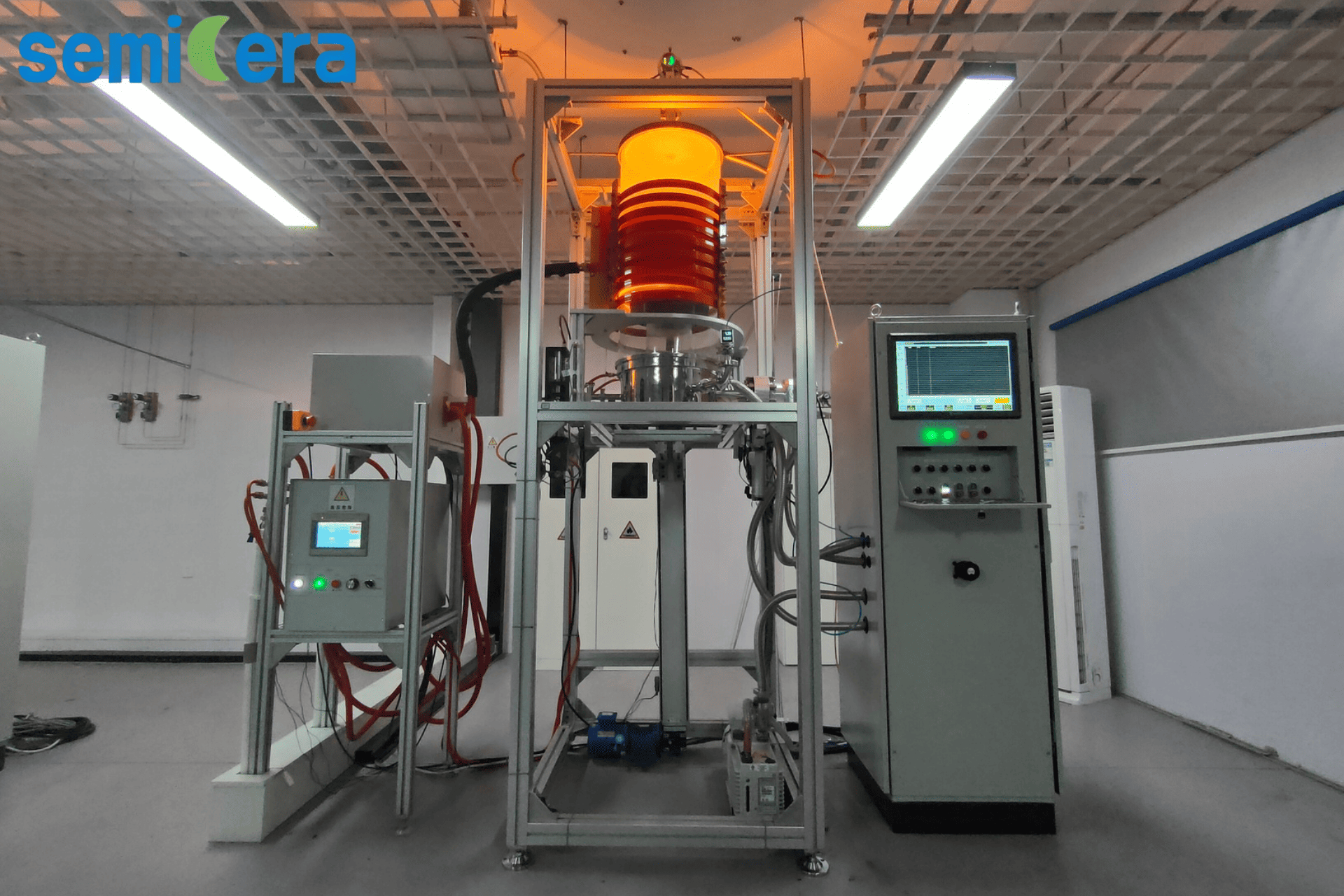
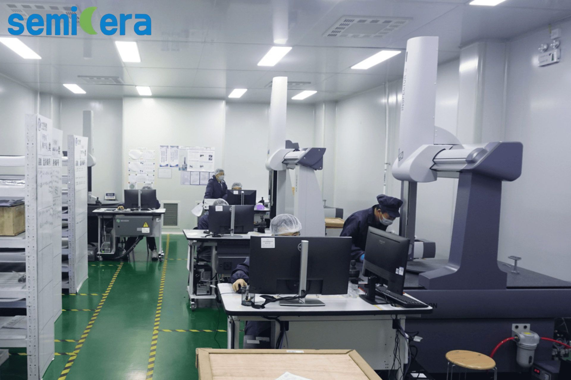
The material definition is only part of the decision. The supplier must be able to control quality at scale. Semicera’s quality system includes a testing center, high-temperature simulation tests, and strict thermal cycle screening to control coating and material cracking risks. Buyers should ask for evidence of this capability during supplier qualification.
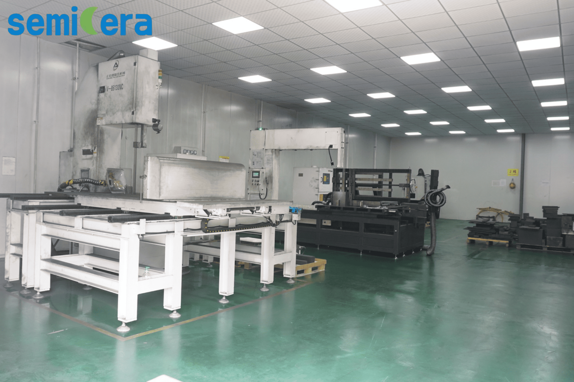
Semicera was founded in 2015 and operates a 40,000 m² facility in Ningbo, China, with over 600 employees. The company reports an annual output of 120,000 units, supported by two research centers, three production bases, and more than 50 advanced production lines. More than 25% of the workforce is dedicated to R&D, with over 100 engineers focused on semiconductor process materials, coating technology, and quality systems.
Use Cases: Where Each Material Choice Works Best
Silicon Crystal Growth
For silicon ingot pulling or crystal growth furnaces, CFC material is the more suitable choice. Its extended lifespan, higher structural load capacity, and up to 50% energy saving translate directly into lower cost per grown crystal.
Epitaxy and MOCVD
For epitaxial reactors and MOCVD systems, SiC/TaC-coated components such as susceptors provide the surface purity and uniformity that epi growth requires. The ultra-pure CVD SiC coating prevents outgassing and particle contamination, and the 10–15% uniformity improvement supports tighter process windows.
High-Temperature Furnace Components
Quartz parts, SiC wafer boats, and graphite components are used across multiple furnace types. The selection criteria remain the same: verify purity, coating quality, and thermal stability. Semicera’s high-purity graphite components are specified with impurity levels below 5 ppm.
Comparison Table: Quick Decision Reference
| Metric | CFC Material vs Conventional Solid Graphite | SiC/TaC-Coated Parts vs OEM Parts |
|---|---|---|
| Service life | 3 to 5 times longer | Same as OEM |
| Structural load capacity | Over 20% higher | Not specified in source data |
| Energy efficiency | Up to 50% better | Not specified in source data |
| Purchase cost | Similar to conventional solid graphite | 30–40% lower than OEM |
| Epitaxial layer uniformity | Not specified in source data | 10–15% improvement |
| Particle generation | Not specified in source data | Less than 5% |
| Defect density | Not specified in source data | Minimized; ultra-pure CVD SiC coating prevents outgassing and particle contamination |
| Maintenance | Reduced due to better lifespan | Identical service cycle and maintenance interval as OEM |
| Best suited for | Silicon crystal growth process | Epi process |
FAQ: Semiconductor Process Material Purchasing Questions
What purity and quality benchmarks should be verified before approving a semiconductor process material?
Buyers should verify impurity levels, coating integrity, and thermal stability. Semicera’s high-purity graphite components are specified with impurity levels below 5 ppm. To manage coating and material cracking risks, Semicera applies high-temperature simulation tests and strict thermal cycle screening before shipment.
Does Semicera supply both CFC materials and SiC/TaC-coated components?
Yes. Semicera (Ningbo Miami Advanced Material Technology Co., LTD) supplies CVD SiC coating parts, CVD TaC coating parts, CVD PyC coating parts, SiC ceramic parts, semiconductor advanced ceramic parts, quartz parts, carbon fiber parts, and CFC material. The product range also includes SiC-coated graphite susceptors, TaC-coated diversion rings, SiC wafer boats, semiconductor quartz parts, and hot-zone components. The company operates more than 50 advanced production lines across three production bases, supported by two research centers and over 100 R&D engineers.
Can SiC/TaC-coated parts reduce costs compared with OEM parts without sacrificing lifespan?
Yes. According to Semicera’s comparison data, SiC/TaC-coated parts are 30–40% lower in price than OEM parts while providing the same lifespan and identical service cycles. The parts also deliver a 10–15% improvement in epitaxial layer uniformity and less than 5% particle generation. This combination can reduce both component cost and defect-related losses.
Can I request a sample or trial batch to validate the material in my process?
To discuss a sample or trial batch, contact Semicera’s sales team at sales05@semi-cera.com or WhatsApp +86 15957878134. Provide your process conditions, target component, and required specifications so the team can confirm the right coating and grade for evaluation.
What lead time and supply commitment should I expect?
Lead time depends on the component type, coating specification, and order volume. Semicera’s production system includes raw material warehousing, semi-finished processing stations, and finished goods storage, with an annual output of 120,000 units. For current lead times and supply planning, contact the sales team directly.
Conclusion and Next Step
The decision between CFC material, conventional solid graphite, and SiC/TaC-coated components should be based on process requirements, not general preference. For silicon crystal growth, CFC material offers longer life, higher structural capability, and meaningful energy savings. For epitaxy and MOCVD, SiC/TaC-coated parts offer lower cost, equal lifespan, and measurable process improvements compared with OEM parts.
The supplier qualification step is equally important. Verify impurity levels, thermal testing, and quality-control systems before approving a material source.
Next step: To compare material options for your process, contact Semicera’s team at www.semi-cera.com. Request the product catalog to review coating options, component specifications, and manufacturing capabilities.
Have Questions or Need More Details?
Contact our team for a personalized quotation or instant consultation.
Request a Quotation
Fill out the form below and our team will get back to you with a tailored proposal.
WhatsApp Direct Chat
Prefer to chat in real-time? Message us on WhatsApp for instant assistance & quick answers.
- Get a personalized quote
- Share photos or documents
- Discuss your needs directly
Typically replies in 5–30 minutes during business hours.