Semicera Semiconductor Process Materials: A 2026 Company and Supplier Assessment
Semicera Semiconductor Process Materials: A 2026 Company and Supplier Assessment
.jpg)
Semiconductor process materials are the high-purity materials and components placed inside wafer-processing equipment: susceptors, wafer boats, furnace tubes, etch rings, insulation felts, heaters, and crucibles. They must control thermal behavior, resist process chemistry, and keep metal contamination extremely low. This article is a company analysis of Semicera (Ningbo Miami Advanced Material Technology Co., Ltd.) for engineers, procurement teams, and suppliers who need to understand whether Semicera is a suitable partner for epitaxy, etch, diffusion, oxidation, and crystal growth equipment.
Company Overview: Semicera at a Glance
Semicera (Ningbo Miami Advanced Material Technology Co., Ltd.), established in 2015, designs and manufactures high-purity semiconductor materials and components. It operates dual research centers and three large-scale production bases, employs more than 600 people, and runs a 40,000 m² manufacturing facility. The company reports more than 50 advanced production lines, an annual output of 120,000 units, and an export share of about 40 percent, with main markets in the EU, USA, and Asia.
The product portfolio covers CVD SiC coating parts, CVD TaC coating parts, CVD PyC coating parts, SiC ceramic parts, semiconductor advanced ceramic parts, quartz parts, carbon fiber parts, and CFC material. These products are used in LED, IC integrated circuits, third-generation semiconductors, epitaxy, MOCVD, CVD, and photovoltaic applications.
Semicera lists SiC-coated graphite susceptors, TaC-coated diversion rings, SiC wafer boats, semiconductor quartz parts, and high-purity graphite components with impurity levels below 5 ppm as its flagship products. This range is relevant because many semiconductor processes require a combination of hot-zone insulation, structural carbon, coated graphite, and quartz consumables.
Why the Choice of Semiconductor Process Materials Is Difficult
A process material failure is not only a component failure. It can generate particles, introduce metals, change thermal uniformity, or shorten preventive maintenance cycles. In etch, components are exposed to fluorine- and chlorine-based plasma. In epitaxy, carriers operate above 1600°C in ammonia and hydrogen. In crystal growth, hot-zone materials must survive ultra-pure vacuum conditions over 2000°C. Buyers therefore need more than a material grade; they need a supplier that can translate process requirements into controlled purity, coating, and dimensional specifications.
This is especially true for semiconductor graphite parts, CFC material, CVD SiC coatings, TaC coatings, and quartz components. Small variations in ash content, coating thickness, or surface finish can change the behavior of a furnace or etch chamber. Supplier selection therefore becomes a technical evaluation rather than a simple purchase decision.
Industry Background: Demand Keeps Moving Toward High-Purity Components
The global semiconductor materials market reached $67.5 billion in 2024, up 3.8 percent from 2023, according to SEMI. Wafer fabrication materials revenue, which includes process chemicals and CVD materials, increased 3.3 percent to $42.9 billion. In specialized segments, Verified Market Reports estimated the semiconductor graphite market at about $1.62 billion in 2024 with a projected CAGR of 7.2 percent through 2032. Valuates Reports estimated the SiC-coated graphite susceptor market at roughly $350 million in 2024. TECHCET sized the global market for quartz fabricated parts used in semiconductor manufacturing at about $2.21 billion in 2024.
One technical trend is the growing use of coatings. CVD SiC coating is the dominant protection method for graphite susceptors in MOCVD and epitaxial reactors because of its high purity and thermal conductivity. TaC coatings are also relevant for ultra-high-temperature processes. This environment favors suppliers that can combine graphite purification, machining, coating, and quartz processing under one roof.
Detailed Solution: Semicera’s Product Portfolio and Technical Capabilities
High-Purity Graphite and Hot-Zone Materials
Semiconductor graphite is one of Semicera’s core material platforms. It is supplied as high-purity isostatic graphite blocks or machined parts with ultra-fine grain size of 2–5 µm, ash content ≤5 ppm, flexural strength of 45–65 MPa, and coefficient of thermal expansion of 4.0–4.6×10⁻⁶ K⁻¹. These properties make the material suitable for hot-zone and process components that require high thermal conductivity, high-temperature resistance, and machinability.
For crystal growth furnaces, Semicera supplies CFC material, a carbon-carbon composite with a 2.5D or 3D needle-punched carbon fiber matrix. It is used for heaters, bolts, crucibles, and other structural hot-zone components. Tensile strength ranges from 90 to 140 MPa, bulk density from 1.65 to 1.78 g/cm³, and ash content is ≤10 ppm after halogen purification.
Semicera also produces semiconductor soft felt and semiconductor rigid felt. The soft felt is a flexible purified graphite insulation roll with carbon content ≥99.99 percent, tensile strength of 0.12–0.25 MPa, moisture absorption below 1.0 percent after purification, and standard thicknesses of 3 mm, 5 mm, and 10 mm. The rigid felt is a purified carbon rigid board with ash content ≤20 ppm (ultra grade ≤5 ppm), thermal conductivity of 0.15–0.35 W/m·K at 1500°C, and processing temperature up to 2500°C in inert vacuum.
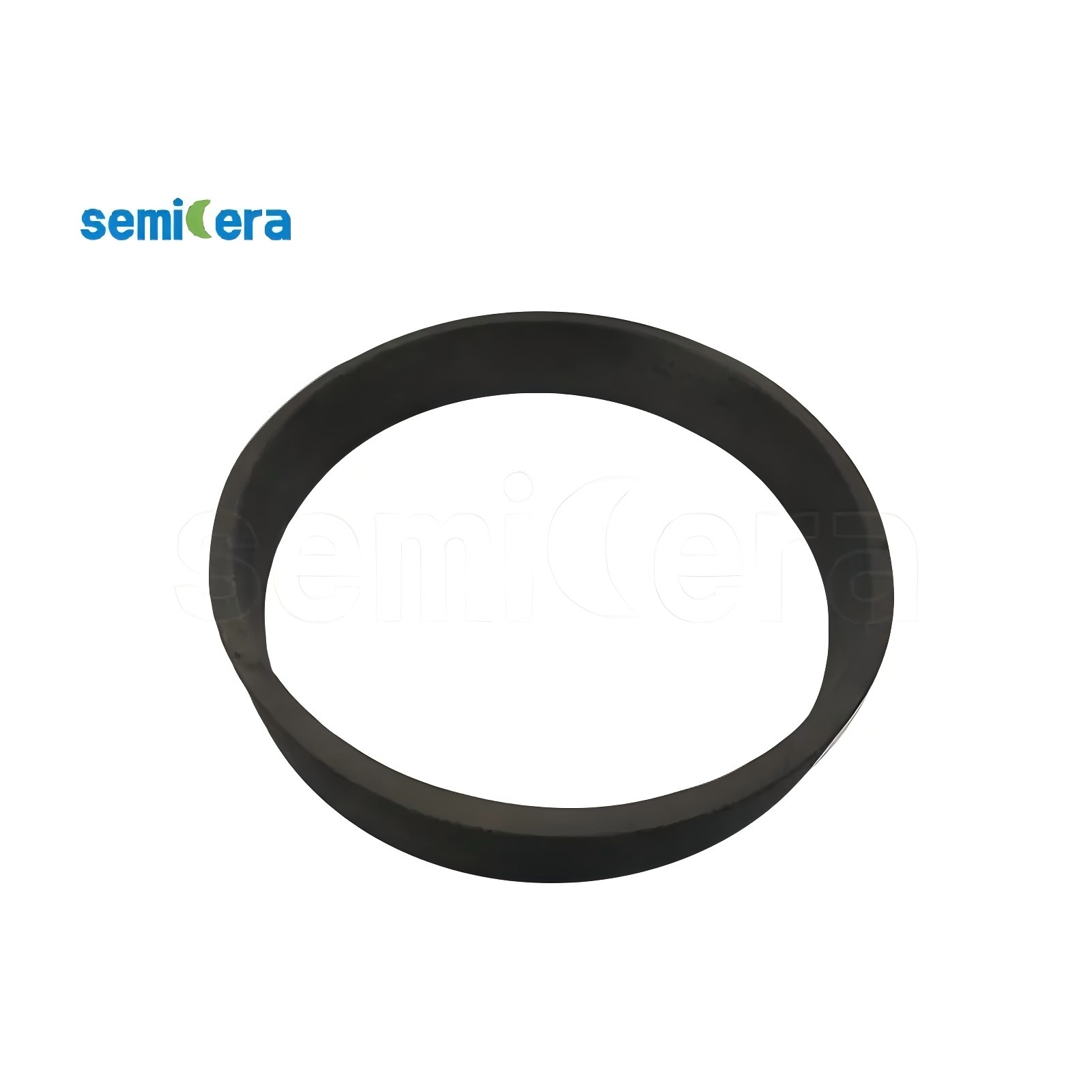
CVD SiC, TaC, and PyC Coated Components
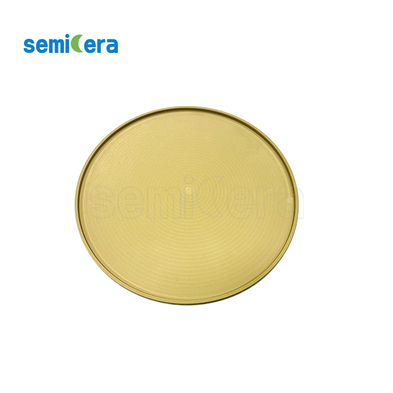
Coating technology is central to Semicera’s product line. The CVD SiC coating graphite carrier (CVD-01) is a MOCVD multi-pocket wafer susceptor or tray designed for epitaxy and RTP processes. The carrier has a typical coating thickness of 100 µm, a range of 50–150 µm, purity of 99.99995 percent, Vickers hardness of 2500, and an FCC beta-phase polycrystal structure with (111) orientation.
The CVD TaC coating graphite carrier (CVD-02) uses a cubic tantalum carbide (TaC) matrix coating on a CVD SiC + graphite substrate. Coating thickness is typically 25–45 µm, maximum operating temperature reaches up to 2200°C, and the coating has outstanding resistance to ammonia and hydrogen etching. The product is used in semiconductor epitaxy processes, including ultra-high-temperature SiC/GaN epitaxial reactors and advanced MOCVD systems.
In addition to SiC and TaC, Semicera offers CVD PyC coating parts. The PyC-coated family is part of the broader semiconductor hot-zone and process component portfolio.
SiC Ceramics and Bulk CVD SiC Parts
For etch process applications, Semicera supplies an etch ring, classified as a focus ring or edge ring for plasma etchers. It is made from pure CVD solid SiC or high-purity silicon single crystal. Flatness tolerance is ≤10 µm, total metal purity is below 5 ppb, and the plasma erosion rate is less than 2 nm/min under high-density CF4/O2 plasma.
The CVD solid SiC part (CVD-03) is a bulk silicon carbide process component or dummy wafer made from 100 percent bulk solid CVD SiC with zero substrate. Density is ≥3.21 g/cm³, thermal conductivity is ≥150 W/m·K, and porosity is 0 percent. These parts are used in SiC crystal growth and plasma-facing environments.
For crystal growth raw material, the CVD SiC particle (CVD-04) offers purity of ≥99.9999 percent, total metals below 1 ppm, free carbon ≤0.05 ppm, and grain sizes from 1.0 to 5.0 mm. It is used as a high-purity PVT SiC crystal growth raw material.
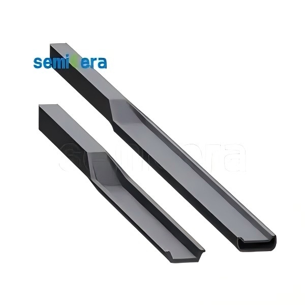
The SiC wafer boat (SiC-01) is a recrystallized or sintered silicon carbide diffusion boat for oxidation and diffusion processes. Maximum working temperature is 1600°C, thermal shock resistance supports cycling from 1000°C to room temperature, and service life is more than five times that of traditional quartz boats. The SiC furnace tube (SiC-02) is made with CVD SiC coating on a SiSiC substrate, is impermeable to gases under vacuum, has wall thickness uniformity within ±0.2 mm, and can be supplied up to 3000 mm long. The SiC paddle (SiC-03) is an automated cantilever loader for diffusion furnaces with load capacity up to 15 kg above 1100°C and deflection ≤2.0 mm at maximum reach.
Quartz and Fused-Silica Components
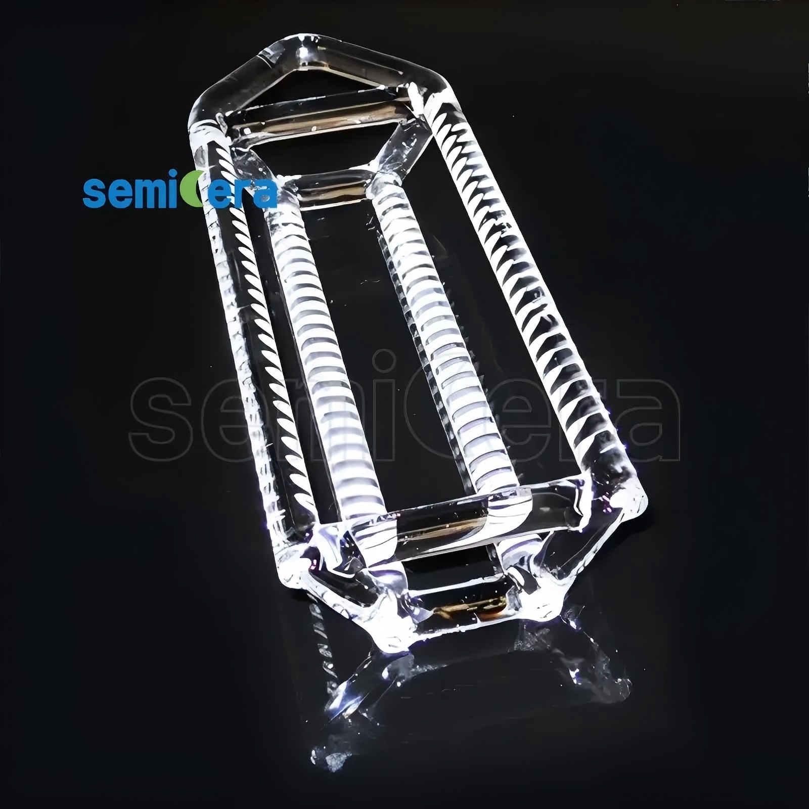
Semicera also covers semiconductor quartz parts. The quartz furnace tube is a high-purity fused quartz process tube or reaction chamber with hydroxyl content below 20 ppm, low-hydroxyl grade below 5 ppm, outer diameter tolerance ±1.0 percent, bubble and inclusion-free surface, and optimized sagging resistance for vertical or horizontal orientations. It is used in annealing and diffusion processes.
The quartz wafer boat is a diffusion or oxidation batch wafer carrier made from ultra-high-purity fused quartz, GE214 or equivalent, with SiO2 purity ≥99.99 percent. Slot pitch tolerance is ≤±0.05 mm, continuous operating temperature is 1150°C, and short-term operation is possible up to 1300°C.
Comparison Table: Semicera Material Families and Typical Applications
Buyers can use this table as an initial screening tool. All values are taken from Semicera’s published product specifications.
| Material Family | Typical Components | Key Verified Specifications | Representative Use |
|---|---|---|---|
| High-purity isostatic graphite | Blocks, machined parts | Ash ≤5 ppm; grain 2–5 µm; flexural strength 45–65 MPa; CTE 4.0–4.6×10⁻⁶ K⁻¹ | Hot-zone structures, susceptor basements, process components |
| CFC material | Heaters, bolts, crucibles | Tensile strength 90–140 MPa; density 1.65–1.78 g/cm³; ash ≤10 ppm after halogen purification | Silicon and silicon carbide crystal growth |
| Semiconductor soft felt | Flexible insulation rolls | Carbon ≥99.99%; tensile strength 0.12–0.25 MPa; thickness 3/5/10 mm | Hot-zone thermal insulation |
| Semiconductor rigid felt | Insulation boards, rings | Ash ≤20 ppm, ultra ≤5 ppm; thermal conductivity 0.15–0.35 W/m·K at 1500°C; processing to 2500°C | Crystal growth furnace insulation barriers |
| CVD SiC-coated graphite | MOCVD susceptors, trays | Coating 50–150 µm, typical 100 µm; purity 6N; hardness 2500 Vickers | Epitaxy, RTP, SiC crystal growth |
| CVD TaC-coated graphite | MOCVD susceptors, trays | Coating 25–45 µm; max operating temperature 2200°C; NH3/H2 etching resistance | High-temperature epitaxy, SiC/GaN MOCVD |
| CVD solid SiC | Process components, dummy wafers | Density ≥3.21 g/cm³; thermal conductivity ≥150 W/m·K; zero porosity | Plasma etch, SiC crystal growth |
| SiC wafer boat | Diffusion boat | Max working temperature 1600°C; service life >5 times quartz boats | Oxidation, diffusion, LPCVD |
| Fused quartz | Furnace tube, wafer boat | OH <20 ppm; SiO2 ≥99.99%; slot pitch tolerance ≤±0.05 mm | Oxidation, diffusion, annealing |
Step-by-Step: How to Qualify Semicera for Your Process Material Requirements
- Define the process window. Identify the relevant process: epitaxy, etch, oxidation, diffusion, LPCVD, RTP, or silicon and silicon carbide crystal growth. Record maximum temperature, gas chemistry, vacuum condition, and wafer loading method.
- Select the material family. Use the comparison table to narrow options. For example, a 1600°C oxidation process may point to SiC wafer boats, while a 1150°C process may allow quartz boats.
- Check purity and coating parameters. Verify graphite ash content, CVD SiC purity, TaC coating thickness, quartz hydroxyl content, and total metal impurities. For Semicera, key parameters include graphite ash ≤5 ppm, CVD SiC purity 6N, TaC coating 25–45 µm, and etch ring total metal <5 ppb.
- Review manufacturing capabilities. Evaluate whether the supplier controls machining, coating, purification, and quality inspection. Semicera operates dual research centers, three production bases, more than 50 production lines, and a 40,000 m² facility.
- Request samples and run qualification. Confirm dimensional tolerances, coating uniformity, and surface condition. For RTP and epitaxy parts, also confirm no coating peeling under thermal cycling.
- Plan scale-up and supply. Align order volumes with production capacity and regional logistics. Semicera’s annual output is reported at 120,000 units, with about 40 percent of sales exported to the EU, USA, and Asia.
Use Cases: How Semicera Materials Map to Specific Processes
Semiconductor Epitaxy and MOCVD
For epitaxy production, the CVD TaC coating graphite carrier meets ultra-high-temperature conditions of 1600–2200°C in ammonia and hydrogen environments. The material provides high-temperature stability, chemical resistance, and contamination control, with zero carbon outgassing and CTE matched to graphite. The CVD SiC coating graphite carrier is used in epitaxy and RTP processes, protecting wafers, improving thermal uniformity, and supporting 6N purity with no coating peeling under thermal cycling.
Plasma Etch
In etch applications, the etch ring and CVD solid SiC parts protect chamber components, control plasma distribution, improve etch uniformity, and reduce particle contamination. They operate in RF-induced reactive ion etching environments and are specified for high resistance to fluorine and chlorine gases, with total metal impurity below 5 ppb.
Oxidation, Diffusion, and LPCVD
In oxidation and diffusion lines, SiC wafer boats, SiC furnace tubes, quartz furnace tubes, quartz wafer boats, and SiC paddles cover different temperature ranges. SiC boats work up to 1600°C, quartz boats run continuously at 1150°C, and the SiC furnace tube can be built up to 3000 mm for large LPCVD systems.
Silicon and Silicon Carbide Crystal Growth
In crystal growth, Semicera supplies graphite hot-zone materials, CFC structural parts, soft and rigid insulation, and CVD SiC particles. These materials support high-vacuum conditions above 2000°C, ultra-low ash levels, thermal shock resistance, and consistent raw material grain size for PVT growth.
Application profiles documented by Semicera include wafer substrate manufacturing in Japan and China, semiconductor device manufacturing in the United States and Singapore, epitaxy production in Taiwan, etch processes in South Korea, and semiconductor manufacturing in Germany.
Manufacturing, R&D, and Quality Control Capabilities
From a supplier evaluation perspective, Semicera’s manufacturing system is one of its main differentiators. The company operates dual research centers and three large-scale production bases. Its 40,000 m² facility employs roughly 600 people, and the company states that more than 25 percent of its workforce is dedicated to research and development. The R&D focus covers advanced semiconductor process materials, precision manufacturing, coating technologies, and quality control systems.
The production process covers raw material warehousing, graphite machining, coating, processing stations, finished parts warehousing, and quality inspection. This integration is relevant because it gives buyers a single supplier responsible for purification, machining, and coating rather than a trader who assembles components from multiple subcontractors.
Market Position and International Presence
Semicera exports approximately 40 percent of its production, with main markets in the EU, USA, and Asia. Its documented application profiles cover wafer substrate manufacturing in Japan and China, semiconductor device manufacturing in the United States and Singapore, epitaxy production in Taiwan, etch processes in South Korea, and semiconductor manufacturing in Germany. In industry directories, Semicera is identified as a manufacturer and supplier of advanced coatings including TaC and SiC coatings.
This analysis does not include unverified customer names, market share rankings, or revenue figures. Buyers should treat Semicera’s value proposition as a documented manufacturing and specification capability rather than a claim based on testimonials.
Core Strengths Relevant to Buyers
- Portfolio breadth: Semicera covers high-purity graphite, CFC material, soft and rigid felt, CVD SiC and TaC coatings, CVD PyC coatings, SiC ceramics, and quartz components.
- Coating and purity control: The product line includes 6N CVD SiC coatings, TaC coatings for 2200°C operation, and graphite with ash content ≤5 ppm.
- Thermal process coverage: Products are designed for oxidation, diffusion, LPCVD, RTP, epitaxy, etch, and silicon carbide crystal growth.
- Manufacturing integration: Dual research centers, three production bases, more than 50 production lines, and a 40,000 m² facility support scale and consistency.
- Customization potential: Several products are available as machined parts or with customizable dimensions, such as SiC furnace tubes up to 3000 mm long.
- Export experience: About 40 percent of sales go to the EU, USA, and Asia, which is relevant for global fab and equipment supply chains.
Frequently Asked Questions
What purity and specification checks should a buyer perform on Semicera’s semiconductor process materials?
For semiconductor graphite, verify ash ≤5 ppm, grain size 2–5 µm, flexural strength 45–65 MPa, and CTE of 4.0–4.6×10⁻⁶ K⁻¹. For CVD SiC-coated parts, verify 6N purity and coating thickness, typically 50–150 µm with 100 µm standard for the CVD-01 carrier. For TaC-coated carriers, check coating thickness of 25–45 µm and maximum working temperature of 2200°C. For quartz components, check hydroxyl content below 20 ppm and slot pitch tolerance ≤±0.05 mm.
Which semiconductor processes do Semicera materials support?
Semicera’s product lines cover oxidation, diffusion, LPCVD, epitaxy, RTP, etch, and silicon or silicon carbide crystal growth. Documented application regions include the United States, South Korea, Japan, Taiwan, Germany, China, and Singapore. The portfolio includes graphite hot-zone components, CFC heaters and crucibles, SiC wafer boats, furnace tubes, quartz carriers, etch rings, CVD SiC particles, and susceptors.
How should buyers compare material options such as quartz, graphite, CFC, and SiC-coated parts?
Compare by process temperature, gas chemistry, contamination requirements, and component life. Quartz wafer boats operate continuously at 1150°C; SiC wafer boats operate up to 1600°C and have more than five times the service life of traditional quartz boats. CFC and graphite are selected for hot-zone structures, while CVD SiC and TaC coatings add protection in aggressive epitaxy environments. The right choice depends on whether the objective is initial component cost, operating lifetime, or both.
Can Semicera support sample requests and custom parts for qualification?
Semicera produces graphite and quartz parts as machined components with customizable dimensions, and its process-specific application profiles include custom production scenarios. Buyers should request the product catalog and contact Semicera directly to confirm sample availability, dimensional requirements, and qualification procedures.
What should a buyer consider when planning supply from Semicera?
Semicera operates a 40,000 m² facility with three production bases and reports an annual output of 120,000 units. Export business accounts for about 40 percent of sales, with main markets in the EU, USA, and Asia. For long-term planning, buyers should verify current lead times, minimum order quantities, and qualification schedules with Semicera’s sales team.
Conclusion: Sourcing Implications and Future Outlook
Semicera is positioned as a vertically integrated process material manufacturer serving high-temperature semiconductor processes. For buyers, the main sourcing advantage is the ability to specify from one portfolio: high-purity graphite, CFC material, soft and rigid insulation, SiC and TaC coated components, CVD SiC parts, and quartz consumables. Publicly available data shows a 40,000 m² facility, more than 600 employees, dual research centers, an annual output of 120,000 units, and a 40 percent export share.
The company is most relevant for engineering teams that need documented purity levels, coating-based component life, and custom dimensioning. As the global semiconductor materials market expands, suppliers with this type of integrated manufacturing coverage are likely to become more important for epitaxy, etch, diffusion, and crystal growth equipment.

Next step: Review Semicera’s full product specifications in the company catalog or contact the sales team to discuss sample, quotation, and qualification requirements.
Email: sales05@semi-cera.com | Tel/WhatsApp: +86 15957878134
Market data cited: SEMI, Verified Market Reports, Valuates Reports, TECHCET, and Dataintelo. Product data is based on Semicera published specifications.
Have Questions or Need More Details?
Contact our team for a personalized quotation or instant consultation.
Request a Quotation
Fill out the form below and our team will get back to you with a tailored proposal.
WhatsApp Direct Chat
Prefer to chat in real-time? Message us on WhatsApp for instant assistance & quick answers.
- Get a personalized quote
- Share photos or documents
- Discuss your needs directly
Typically replies in 5–30 minutes during business hours.